- 您现在的位置:买卖IC网 > Sheet目录19093 > FQA90N15 (Fairchild Semiconductor)MOSFET N-CH 150V 90A TO-3P
�� �
�
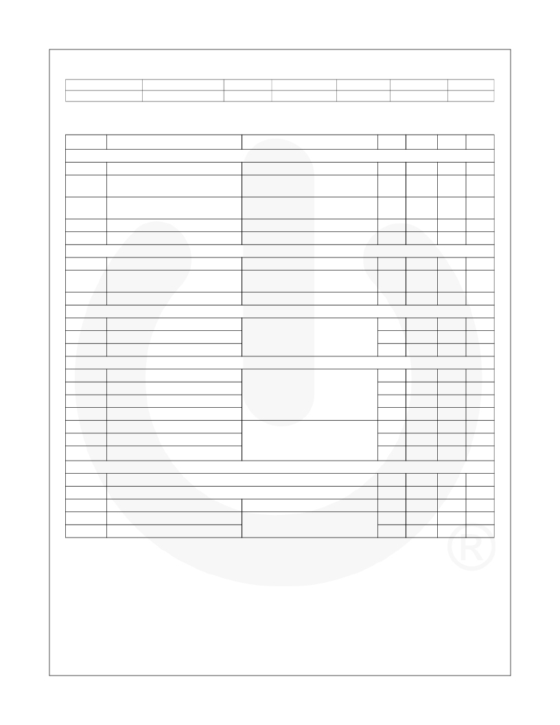
�Package� Marking� and� Ordering� Information�
�Part� Number�
�FQA90N15�
�Top� Mark�
�FQA90N15�
�Package�
�TO-� 3PN�
�Packing� Method�
�Tube�
�Reel� Size�
�N/A�
�Tape� Width�
�N/A�
�Quantity�
�30� units�
�Electrical� Characteristics�
�T� C� =� 25°C� unless� otherwise� noted� .�
�Symbol�
�Parameter�
�Conditions�
�Min.�
�Typ.�
�Max� Units�
�Off� Characteristics�
�BV� DSS�
�Δ� BV� DSS�
�/� Δ� T� J�
�I� DSS�
�I� GSSF�
�I� GSSR�
�Drain-Source� Breakdown� Voltage�
�Breakdown� Voltage� Temperature�
�Coefficient�
�Zero� Gate� Voltage� Drain� Current�
�Gate-Body� Leakage� Current,� Forward�
�Gate-Body� Leakage� Current,� Reverse�
�V� GS� =� 0V,� I� D� =� 250� μ� A�
�I� D� =� 250� μ� A,� Referenced� to� 25� °� C�
�V� DS� =� 150V,� V� GS� =� 0V�
�V� DS� =� 120V,� T� C� =� 150� °� C�
�V� GS� =� 25V,� V� DS� =� 0V�
�V� GS� =� -25V,� V� DS� =� 0V�
�150�
�--�
�--�
�--�
�--�
�--�
�--�
�0.15�
�--�
�--�
�--�
�--�
�--�
�--�
�1�
�10�
�100�
�-100�
�V�
�V/� °� C�
�μ� A�
�μ� A�
�nA�
�nA�
�On� Characteristics�
�V� GS(th)�
�R� DS(on)�
�g� FS�
�Gate� Threshold� Voltage�
�Static� Drain-Source�
�On-Resistance�
�Forward� Transconductance�
�V� DS� =� V� GS� ,� I� D� =� 250� μ� A�
�V� GS� =� 10V,� I� D� =� 45A�
�V� DS� =� 40V,� I� D� =� 45A�
�2.0�
�--�
�--�
�--�
�0.014�
�68�
�4.0�
�0.018�
�--�
�V�
�Ω�
�S�
�Dynamic� Characteristics�
�C� iss�
�C� oss�
�C� rss�
�Input� Capacitance�
�Output� Capacitance�
�Reverse� Transfer� Capacitance�
�V� DS� =� 25V,� V� GS� =� 0V,�
�f� =� 1.0MHz�
�--�
�--�
�--�
�6700�
�1400�
�200�
�8700�
�1800�
�260�
�pF�
�pF�
�pF�
�Switching� Characteristics�
�t� d(on)�
�t� r�
�t� d(off)�
�t� f�
�Q� g�
�Q� gs�
�Q� gd�
�Turn-On� Delay� Time�
�Turn-On� Rise� Time�
�Turn-Off� Delay� Time�
�Turn-Off� Fall� Time�
�Total� Gate� Charge�
�Gate-Source� Charge�
�Gate-Drain� Charge�
�V� DD� =� 75V,� I� D� =� 90A�
�R� G� =� 25� Ω�
�V� DS� =� 120V,� I� D� =� 90A�
�V� GS� =� 10V�
�(Note� 4)�
�(Note� 4)�
�--�
�--�
�--�
�--�
�--�
�--�
�--�
�105�
�760�
�470�
�410�
�220�
�43�
�110�
�220�
�1500�
�950�
�830�
�285�
�--�
�--�
�ns�
�ns�
�ns�
�ns�
�nC�
�nC�
�nC�
�Drain-Source� Diode� Characteristics� and� Maximum� Ratings�
�I� S�
�I� SM�
�Maximum� Continuous� Drain-Source� Diode� Forward� Current�
�Maximum� Pulsed� Drain-Source� Diode� Forward� Current�
�--�
�--�
�--�
�--�
�90�
�360�
�A�
�A�
�V� SD�
�t� rr�
�Q� rr�
�Drain-Source� Diode� Forward� Voltage�
�Reverse� Recovery� Time�
�Reverse� Recovery� Charge�
�V� GS� =� 0V,� I� S� =� 90A�
�V� GS� =� 0V,� I� S� =� 90A�
�dI� F� /dt� =100A/� μ� s�
�--�
�--�
�--�
�--�
�175�
�0.97�
�1.5�
�--�
�--�
�V�
�ns�
�μ� C�
�NOTES:�
�1.� Repetitive� r� ating:� p� ulse� -� width� limited� by� maximum� junction� temperature� .�
�2.� L� =� 0.� 29� mH,� I� AS� =� 9� 0� A,� V� DD� =� 25� V,� R� G� =� 25� Ω� ,� s� tarting� T� J� =� 25� °� C� .�
�3.� I� SD� ≤� 9� 0� A,� di/dt� ≤� 3� 00� A/� μ� s,� V� DD� ≤� BV� DSS� ,� s� tarting� T� J� =� 25� °� C� .�
�4.� Essentially� i� ndependent� of� o� perating� t� emperature� t� ypical� c� haracteristics� .�
�?2006� Fairchild� Semiconductor� Corporation�
�FQA90N15� Rev� C1�
�2�
�www.fairchildsemi.com�
�发布紧急采购,3分钟左右您将得到回复。
相关PDF资料
550-1207
LED 5MM RT ANG LOW CUR YEL PCMNT
550-1204
LED 5MM VERT LOW CUR YELLOW PCMT
550-1107
LED 5MM RT ANG LOW CUR RED PCMNT
550-1104
LED 5MM VERT LOW CUR RED PCMNT
550-0504
LED 5MM 5V VERTICAL RED PC MNT
550-0407
LED 5MM RT ANGLE RED PC MNT
550-0807
LED 5MM 5V RT ANGLE YELLOW PCMNT
550-0804
LED 5MM 5V VERTICAL YELLOW PCMNT
相关代理商/技术参数
FQA90N15
制造商:Fairchild Semiconductor Corporation 功能描述:MOSFET N TO-3P
FQA90N15_F109
功能描述:MOSFET 150V 90A N-Chan Power Trench
RoHS:否 制造商:STMicroelectronics 晶体管极性:N-Channel 汲极/源极击穿电压:650 V 闸/源击穿电压:25 V 漏极连续电流:130 A 电阻汲极/源极 RDS(导通):0.014 Ohms 配置:Single 最大工作温度: 安装风格:Through Hole 封装 / 箱体:Max247 封装:Tube
FQA9N50
功能描述:MOSFET 500V N-Channel QFET RoHS:否 制造商:STMicroelectronics 晶体管极性:N-Channel 汲极/源极击穿电压:650 V 闸/源击穿电压:25 V 漏极连续电流:130 A 电阻汲极/源极 RDS(导通):0.014 Ohms 配置:Single 最大工作温度: 安装风格:Through Hole 封装 / 箱体:Max247 封装:Tube
FQA9N90
功能描述:MOSFET 900V N-Channel QFET RoHS:否 制造商:STMicroelectronics 晶体管极性:N-Channel 汲极/源极击穿电压:650 V 闸/源击穿电压:25 V 漏极连续电流:130 A 电阻汲极/源极 RDS(导通):0.014 Ohms 配置:Single 最大工作温度: 安装风格:Through Hole 封装 / 箱体:Max247 封装:Tube
FQA9N90_07
制造商:FAIRCHILD 制造商全称:Fairchild Semiconductor 功能描述:900V N-Channel MOSFET
FQA9N90_F109
功能描述:MOSFET 900V N-Channel QFET RoHS:否 制造商:STMicroelectronics 晶体管极性:N-Channel 汲极/源极击穿电压:650 V 闸/源击穿电压:25 V 漏极连续电流:130 A 电阻汲极/源极 RDS(导通):0.014 Ohms 配置:Single 最大工作温度: 安装风格:Through Hole 封装 / 箱体:Max247 封装:Tube
FQA9N90C
功能描述:MOSFET 900V N-Channel Q-FET RoHS:否 制造商:STMicroelectronics 晶体管极性:N-Channel 汲极/源极击穿电压:650 V 闸/源击穿电压:25 V 漏极连续电流:130 A 电阻汲极/源极 RDS(导通):0.014 Ohms 配置:Single 最大工作温度: 安装风格:Through Hole 封装 / 箱体:Max247 封装:Tube
FQA9N90C_06
制造商:FAIRCHILD 制造商全称:Fairchild Semiconductor 功能描述:900V N-Channel MOSFET